750 Mitchell Road, Newbury Park, California 91320
Phone: (805) 499-0335, Fax: (805) 499-8108
Email: sales@optodiode.com, Website: www.optodiode.com
FEATURES
" Ideal for electron detection
" Large detection area
" 100% internal QE
ELECTRO-OPTICAL CHARACTERISTICS AT 25癈
PARAMETERS
TEST CONDITIONS
MIN
TYP
MAX
UNITS
Active Area
Responsivity, R
Shunt Resistance, Rsh
Reverse Breakdown Voltage, V
R
Capacitance, C
Rise Time
THERMAL PARAMETERS
STORAGE AND OPERATING TEMPERATURE RANGE
Ambient
2
Nitrogen or Vacuum
Maximum Junction Temperature
Lead Soldering Temperature
1
-10?TO 40癈
2
-20癈 TO 80癈
70癈
260癈
1
0.08" from case for 10 seconds.
2
Temperatures exceeding these parameters may create Oxide growth on the active area.
Over time Responsivity to Low energy radiation and wavelengths below 150nm will Be Compromised.
Shipped with temporary cover to protect photodiode and wire bond. Review Opto Diode
Handling Precautions for IRD Detectors
prior to removing cover.
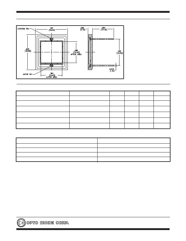
Dimensions are in inch [metric] units.
10mm x 10mm
@ 254nm, V
R
= 0V
V
B
= ?0mV
I
R
= 1礎
V
R
= 0V
V
R
= 0V, R
L
= 50?/DIV>
0.07
20
100
0.08
10
10
0.09
44
10
mm
2
A/W
M-ohm
Volts
nF
usec
ELECTRON DETECTION 100 mm
2
AXUV100G
Revision February 26, 2013
发布紧急采购,3分钟左右您将得到回复。
相关PDF资料
B0205F50200AHF
XFRMR BALUN RF 200-500MHZ 1608
B0310J50100AHF
XFRMR BALUN RF 300-1000MHZ 0805
B0322J5050AHF
XFRMR BALUN RF 300-2200MHZ 0805
B0430J50100AHF
XFRMR BALUN RF 400-3000MHZ 0805
B0809J50ATI
XFRMR BALUN RF 850-915MHZ 0805
B0922J7575A50HF
XFRMR BALUN RF 950-2150MHZ 0805
B0922N7575AHF
XFRMR BALUN RF 950-2150MHZ 0404
BD0205F5050AHF
XFRMR BALUN RF 70-1000MHZ 1608
相关代理商/技术参数
AXUV100TI
制造商:OPTODIODE 制造商全称:OPTODIODE 功能描述:PHOTODIODE 100 mm Square active area
AXUV100TI/C2
制造商:Opto Diode Corp 功能描述:SENSOR ELECTRON DETECTION 100MM
AXUV100TI-C2
制造商:OPTODIODE 制造商全称:OPTODIODE 功能描述:PHOTODIODE 100 mm2
AXUV16 ELG
制造商:Opto Diode Corp 功能描述:SENSOR ELECTRON DETECTION 40DIP
AXUV16ELCS
功能描述:SOCKET CERM FOR AXUV16ELG IRD 制造商:opto diode corp 系列:- 零件状态:有效 配件类型:插口 配套使用产品/相关产品:AXUV16ELG 标准包装:1
AXUV16ELG
制造商:OPTODIODE 制造商全称:OPTODIODE 功能描述:PHOTODIODE 16 ELEMENT 40 pin dual in-line package
AXUV20A
制造商:OPTODIODE 制造商全称:OPTODIODE 功能描述:ELECTRON DETECTION 5.5mm Circular active area
AXUV20ACS
功能描述:SOCKET CERM FOR AXUV20A/UVG20S 制造商:opto diode corp 系列:- 零件状态:有效 配件类型:插口 配套使用产品/相关产品:AXUV20A,AXUV20HS1,SXUV20HS1,UVG20S 标准包装:1